
SUSTAINABLE AI & CRYPTO MINING HARDWARE
DESIGNED IN JAPAN
Lenzo builds ultra-efficient hardware designed for modern parallel workloads — from blockchain to AI inference. Our proprietary CGLA architecture delivers breakthrough performance per watt in a compact, cost-effective form.
INTRODUCING LENZO CORE, BUILT FOR REAL WORKLOADS
Execution, memory, and data flow are coordinated directly in hardware.
This is visible, predictable performance.
This visualization reveals the internal state of LENZO Core, LENZO’s CGLA (Coarse-Grained Linear Array) compute architecture. Each ring represents a scalable CGLA fabric where parallel processing units operate across cascades and memory lanes. Real-time, color-coded states expose execution flow, cache activity, DMA transfers, and external memory interaction. Hardware-level multi-threading and buffering eliminate pipeline stalls, enabling predictable high throughput. LENZO Core delivers scalable performance, energy efficiency, and simplified programming for real-world workloads. Full length demo video available here.
PRODUCTS & SERVICES
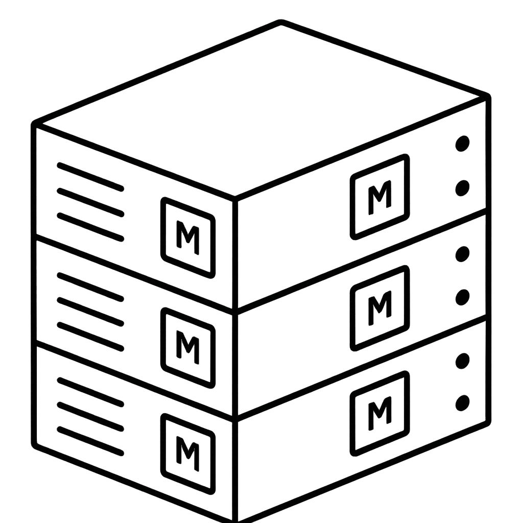
Lenzo M-Series: Crypto Mining Rig
M-Series is built for next-generation mining infrastructure, optimized for SHA256 efficiency and high hashrate-per-watt delivery.
Runs custom ASICs – enabling long-term reliability and simplified 24/7 operation at scale.

Lenzo A-Series: AI Server Platform
Train smarter and run faster—without GPU lock-in.
A-Series is built for next-generation AI infrastructure, optimized for LLM training and inference with ultra-low power draw.
Runs open-source models – enabling flexible deployment and full ownership of your stack.

Technical Consulting Services
We assist with architecture, tuning, and rollout across edge, AI, and blockchain systems.
Whether you’re designing hardware or scaling compute, Lenzo supports every step from chip to deployment.
KEY BENEFITS

High Hash Rate
Outperforms standard ASIC rigs in energy efficiency (J/TH)
Cost-Efficient Hardware
Designed to reduce total cost of ownership over time

Low Power Consumption
Maximizes performance per watt using a novel dataflow architecture

Broad Algorithm Support
Supports SHA256 out of the box; other algorithms can be added upon request

ABOUT
Crafted in Japan, Lenzo is built by the engineers behind some of the world’s fastest chips—from Sony’s PlayStation CPU/GPU teams to the designers of Fujitsu’s supercomputers. Our founding team includes researchers from NAIST and ITRI Taiwan, with deep expertise in large-scale compute infrastructure. We are system architects and builders, committed to engineering high-performance, energy-efficient hardware for a new generation of workloads.
CAREERS
TECHNICAL RESOURCES

EXPLAINER VIDEO: Architecture Leads System Design
NAIST Computing Architecture Lab's Youtube channel published a new video featuring a lecture by LENZO's Co-Founder & Chief Architect , Prof. Yasuhiko Nakashima.
In this talk, Prof. Nakashima shares perspectives on training environments for semiconductor engineers and broader directions for future accelerator technologies, including AI and cryptography.
A central theme of the lecture is the idea that “Architecture Leads System Design,” highlighting how architectural choices shape system-level performance, efficiency, and long-term adaptability. The video is published as a knowledge-sharing resource and is available to watch in full below.

Looking Back at Tech Osaka 2025 - LENZO Exhibition Retrospective
Tech Osaka 2025 provided LENZO with a valuable opportunity to present its technology and build new connections across Japan’s innovation ecosystem, below is retrospective video outlining our experience at the event.
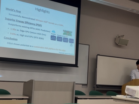
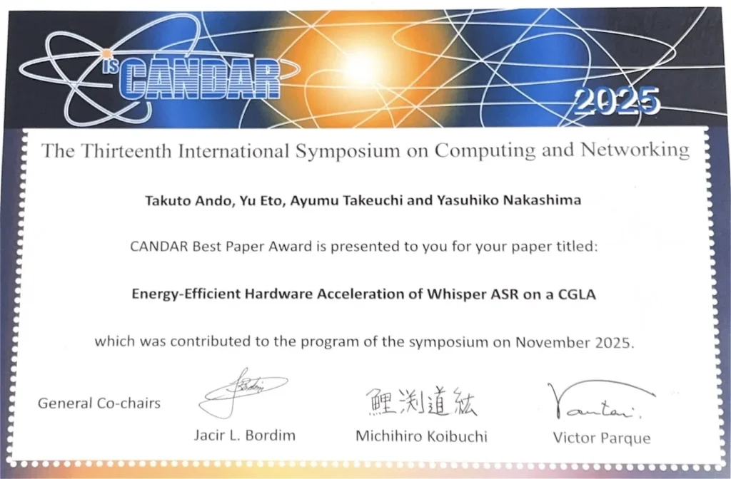
"Energy-Efficient Hardware Acceleration of Whisper ASR on a CGLA" has been selected for the CANDAR Best Paper Award
We are pleased to announce that a paper authored by LENZO's Takuto Ando among others, exploring the core technology of LENZO, "Energy-Efficient Hardware Acceleration of Whisper ASR on a CGLA”, has been selected for The Thirteenth International Symposium on Computing and Networking (CANDAR 2025)'s Best Paper Award during the symposium held in Yamagata from November 25–28, 2025.
CANDAR is a leading international forum covering advanced computing and networking research, spanning theoretical foundations, parallel and distributed systems, hardware architectures, and practical applications. Among numerous submissions, Ando’s work was recognized for its originality, technical contribution, and impact.
Learn more at:
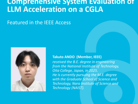
Our CGLA-Based LLM Inference Research Accepted to IEEE Access
We are pleased to share that our collaborative research with NAIST, “Efficient Kernel Mapping and Comprehensive System Evaluation of LLM Acceleration on a CGLA” has been formally accepted to the international journal IEEE Access. You can access the full article for download here.
This work represents the first end-to-end evaluation of Large Language Model (LLM) inference on a non-AI-specialized Coarse-Grained Linear Array (CGLA) accelerator, using the state-of-the-art Qwen3 model family as the benchmark and reinforces the viability of general-purpose CGLA architectures—not just fixed-function ASICs or high-power GPUs—for next-generation LLM inference. It demonstrates that compute efficiency, programmability, and adaptability to changing algorithms can coexist in a reconfigurable architecture.
For LENZO, this is a meaningful milestone in advancing the underlying theory and validation behind our CGLA-based compute vision.
Publication Details
Title:
Efficient Kernel Mapping and Comprehensive System Evaluation of LLM Acceleration on a CGLA
Journal: IEEE Access
DOI: 10.1109/ACCESS.2025.3636266
INVESTORS
Investing in the Future of Intelligent Compute

Oki MatsumotoFounder and Chairman - Monex Group
As the rapid expansion of generative AI accelerates competition in algorithms, a new frontier is emerging in the optimization of computational circuits and energy efficiency. We hold great expectations that Japan-based LENZO will drive a game-changing breakthrough with its innovative semiconductors and establish a strong presence on the global stage.

Takuya HiroseFormer CFO - Remixpoint
LENZO’s core technology, CGLA, is an advanced innovation with the potential to address one of the most pressing challenges in cryptocurrency mining—energy consumption. Just as the PlayStation once transformed the gaming industry with its proprietary semiconductors, we have great expectations that Japan-born LENZO will revolutionize the computational foundation of blockchain and evolve into a world-leading AI semiconductor company.

Narimasa MakinoCEO - Monozukuri Ventures
Serial entrepreneur Kenshin Fujiwara has chosen his next challenge in the rapidly expanding global AI and crypto markets. Building on an architecture developed at Nara Institute of Science and Technology (NAIST), LENZO is developing semiconductor chips tailored for AI and crypto applications. Its vertically integrated business model, which combines Japan’s traditional strengths in hardware and software, is truly unique and holds strong potential to compete on the global stage.
Ready to power the next era of intelligent infrastructure?
