
SUSTAINABLE AI & CRYPTO MINING HARDWARE
DESIGNED IN JAPAN
Lenzo builds ultra-efficient hardware designed for modern parallel workloads — from blockchain to AI inference. Our proprietary CGLA architecture delivers breakthrough performance per watt in a compact, cost-effective form.
INTRODUCING LENZO CORE, BUILT FOR REAL WORKLOADS
Execution, memory, and data flow are coordinated directly in hardware.
This is visible, predictable performance.
This visualization reveals the internal state of LENZO Core, LENZO’s CGLA (Coarse-Grained Linear Array) compute architecture. Each ring represents a scalable CGLA fabric where parallel processing units operate across cascades and memory lanes. Real-time, color-coded states expose execution flow, cache activity, DMA transfers, and external memory interaction. Hardware-level multi-threading and buffering eliminate pipeline stalls, enabling predictable high throughput. LENZO Core delivers scalable performance, energy efficiency, and simplified programming for real-world workloads. Full length demo video available here.
PRODUCTS & SERVICES
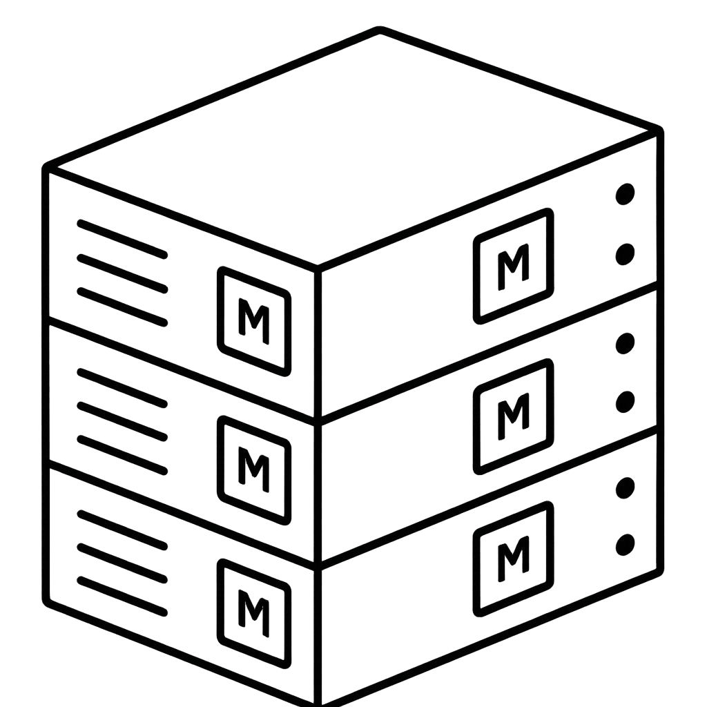
Lenzo M-Series: Crypto Mining Rig
M-Series is built for next-generation mining infrastructure, optimized for SHA256 efficiency and high hashrate-per-watt delivery.
Runs custom ASICs – enabling long-term reliability and simplified 24/7 operation at scale.

Lenzo A-Series: AI Server Platform
Train smarter and run faster—without GPU lock-in.
A-Series is built for next-generation AI infrastructure, optimized for LLM training and inference with ultra-low power draw.
Runs open-source models – enabling flexible deployment and full ownership of your stack.

Technical Consulting Services
We assist with architecture, tuning, and rollout across edge, AI, and blockchain systems.
Whether you’re designing hardware or scaling compute, Lenzo supports every step from chip to deployment.
KEY BENEFITS

High Hash Rate
Outperforms standard ASIC rigs in energy efficiency (J/TH)
Cost-Efficient Hardware
Designed to reduce total cost of ownership over time

Low Power Consumption
Maximizes performance per watt using a novel dataflow architecture
Broad Algorithm Support
Supports SHA256 out of the box; other algorithms can be added upon request

ABOUT
Crafted in Japan, Lenzo is built by the engineers behind some of the world’s fastest chips—from Sony’s PlayStation CPU/GPU teams to the designers of Fujitsu’s supercomputers. Our founding team includes researchers from NAIST and ITRI Taiwan, with deep expertise in large-scale compute infrastructure. We are system architects and builders, committed to engineering high-performance, energy-efficient hardware for a new generation of workloads.
CAREERS
RESOURCES & PRESS
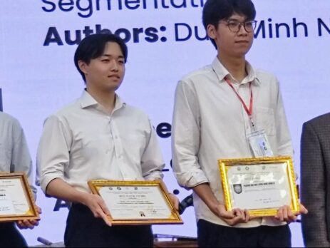
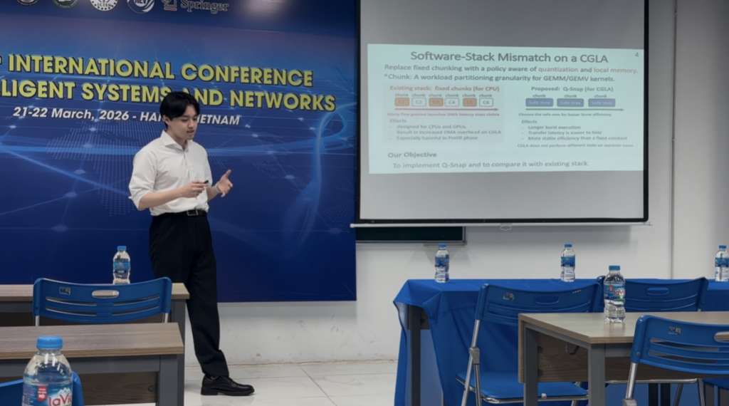
Best Paper Award at ICISN 2026
LENZO’s latest research on CGLA-based LLM inference has received the Best Paper Award at the Sixth International Conference on Intelligent Systems and Networks (ICISN 2026) in Hanoi, Vietnam.
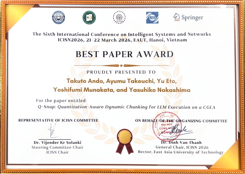
The paper, “Q-Snap: Quantization-Aware Dynamic Chunking for LLM Execution on a CGLA,” was presented by Takuto Ando, Ayumu Takeuchi, Yu Eto, Yoshifumi Munakata, and Yasuhiko Nakashima.
It addresses the fundamental inefficiency of LLM inference on conventional GPU architectures by introducing a hardware-aware scheduling approach optimized for CGLA.
Using an FPGA prototype and 28nm ASIC projections, the method demonstrates both improved performance and higher energy efficiency compared to modern GPU systems.
This work reinforces LENZO’s focus on architecture-driven compute, where efficiency gains are achieved through design and execution - not just process scaling.
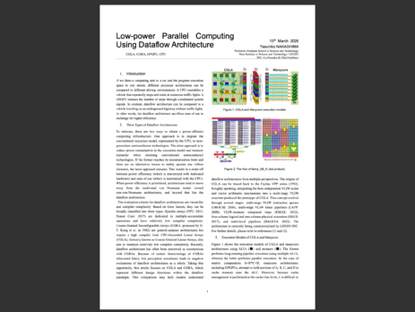
TECHNICAL BRIEF: Low-Power Parallel Computing Using Dataflow Architecture
LENZO Chief Architect and NAIST Professor Yasuhiko Nakashima has published a new article exploring low-power parallel computing using dataflow architectures and their potential to improve performance and energy efficiency for modern workloads.
The paper compares traditional processor designs - including CPUs, GPUs, and "manycore" architectures - with dataflow-based execution models, highlighting how pipeline driven computation can significantly reduce memory bottlenecks and improve power efficiency.
The article also introduces the CGLA architecture, a dataflow computing approach developed through years of research at NAIST and now being commercialized by LENZO. By enabling long-running pipeline execution with predictable memory behavior, CGLA aims to deliver highly efficient computation for emerging workloads such as AI and large-scale numerical processing.

LENZO closes 500M JPY Seed Round with investments from Incubate Fund, Sony Innovation Fund and Mitsubishi UFJ Capital
Funds to be used to produce first ever chips powered by CGLA (Coarse-Grained Linear Array) architecture
Nara, Japan - March 11th, 2026 - LENZO, a Japan-based semiconductor startup building next-generation compute infrastructure, today announced the closing of its 500 million JPY Seed funding round. The round includes investments from Incubate Fund, Sony Innovation Fund, and Mitsubishi UFJ Capital, underscoring strong backing for Japan-originated semiconductor innovation.
The proceeds will be primarily used to produce LENZO’s first proprietary silicon - bringing its CGLA architecture from advanced design into physical chips.Purpose-built for materially higher performance per watt across AI and blockchain workloads, CGLA targets one of computing’s most urgent constraints: energy.

“This round marks our transition from architecture to silicon,” said Kenshin Fujiwara, CEO of LENZO. “Compute demand is accelerating globally, but energy is the bottleneck. Our first chip is designed to prove that next-generation performance can be achieved with dramatically improved power efficiency.”
Investors’ Strong and Strategic Support
Incubate Fund, one of Japan’s leading early-stage venture capital firms, invested based on LENZO’s potential to build a globally competitive semiconductor platform originating from Japan.
Masahiko Homma, Representative Partner at Incubate Fund, said: "The evolution of AI is accelerated not only by software but also by innovation in the computing infrastructure itself. In an era dominated by GPUs, we see great potential and value in the efforts of a Japanese semiconductor design startup challenging new computing architectures."
Sony Innovation Fund, managed by Sony Ventures Corporation, made this investment focusing on the development of next-generation semiconductor and computing technologies.
Kazuhito Hatano, CEO of Sony Ventures Corporation, said: “We see significant value in how LENZO is directly tackling the innovation of computing infrastructure that is essential in the AI era, aiming to commercialize low-power, high-efficiency semiconductor technologies. We are supporting this project as we believe it has great potential to take on the global market as a deep tech originating from Japan and contribute to strengthening industrial competitiveness.”
Mitsubishi UFJ Capital Co., Ltd., the venture capital arm of Mitsubishi UFJ Financial Group, participated in the round as part of its broader commitment to strengthening Japan’s semiconductor ecosystem and supporting high-potential deep-tech ventures.
Shogo Irokawa, Investment Department No.1 Manager, Mitsubishi UFJ Capital Co., Ltd., said: “LENZO’s CGLA architecture is an innovative technology that tackles long‑standing challenges in power efficiency through a uniquely original approach. Advancing from the design phase to physical chip development in this latest step marks an important milestone as the company continues to strengthen its presence in the global market. We sincerely look forward to seeing LENZO, as a semiconductor startup originating from Japan, continue to create new value and achieve further growth.”
Energy-efficient infrastructure for the AI era
AI and blockchain infrastructure is scaling rapidly, driving significant growth in power demand. As energy availability and cost increasingly determine deployment viability, LENZO’s CGLA architecture embeds power awareness directly at the hardware level — enabling more efficient scaling of compute-intensive workloads.
With silicon production underway, LENZO is engaging infrastructure operators, blockchain operators, enterprise customers, and ecosystem partners seeking next-generation power-efficient compute solutions.
About LENZO
LENZO builds ultra-efficient hardware for modern parallel workloads - from blockchain to AI inference. Its proprietary CGLA architecture delivers breakthrough performance per watt in a compact, cost-effective form factor.
For media inquiries or partnership discussions:
Adrian Sossna
Incubate Fund、Sony Innovation Fund、三菱UFJキャピタルより出資を受け、5億円のシードラウンドを完了
〜調達資金は、CGLA(Coarse-Grained Linear Array)アーキテクチャを採用した初のチップ製造に充当〜
次世代計算インフラの構築を目指す半導体スタートアップのLENZO株式会社(本社:奈良県生駒市、代表取締役:藤原健真)は、総額5億円のシードラウンド資金調達を完了したことをお知らせします。本ラウンドには、Incubate Fund、Sony Innovation Fund、三菱UFJキャピタルが参加しており、日本発の半導体イノベーションに対する強力な投資家の支援を示しています。
今回の調達資金は主に、LENZO初の独自シリコンの製造に充当され、CGLAアーキテクチャを高度な設計段階から実際の物理チップへと移行させます。
CGLAは、AIおよびブロックチェーンのワークロードにおいて飛躍的に高い電力効率(Performance per Watt)を実現することを目的に設計されており、コンピューティング分野における最も喫緊の課題の一つである「エネルギー制約」に正面から取り組みます。
LENZOのCEOである藤原健真は、次のように述べています。
「今回のラウンドは、アーキテクチャ段階からシリコン実装への移行を意味します。世界的に計算需要は加速していますが、ボトルネックとなっているのは消費電力です。当社のチップは、劇的に向上した電力効率によって次世代の性能を実現できることを証明するために設計されています。」
強力な投資家および戦略的支援
日本を代表するアーリーステージ・ベンチャーキャピタルであるIncubate Fundは、日本発でグローバル競争力を持つ半導体プラットフォームを構築するLENZOの可能性を評価し、出資を行いました。本間真彦 インキュベイトファンド 代表パートナーは、次のように述べています。
「AIの進化は、ソフトウェアだけでなく、計算基盤そのものの革新によって加速します。GPU一強とも言える時代に、新しい計算アーキテクチャへ挑む日本発の半導体設計スタートアップの取り組みに、大きな可能性とやりがいを感じています。」
ソニーベンチャーズ株式会社が運営するSony Innovation Fundは、次世代半導体および計算技術領域の発展を見据えて本件出資を行いました。代表取締役社長 波多野和人は、次のように述べています。
「LENZOは、AI時代に不可欠となる計算基盤の革新に真正面から取り組み、省電力かつ高効率な半導体技術の実用化を目指している点に大きな意義を感じています。日本発のディープテックとして世界市場への挑戦が期待され、産業競争力の強化にも寄与する可能性が高いと考え支援しています。」
三菱UFJフィナンシャル・グループのベンチャーキャピタル部門である三菱UFJキャピタルは、半導体分野における市場環境の変化とLENZO社の技術的優位性を総合的に評価し、本ラウンドに参加いたしました。三菱UFJキャピタル株式会社 投資第一部 次長 色川将吾は、次のように述べています。
「LENZO社のCGLAアーキテクチャは、電力効率に関する従来の課題に独自のアプローチで挑む革新的な技術であり、設計段階から物理チップの開発へと進む今回のステップは、同社がグローバルで存在感を高めていくうえで重要なマイルストーンになると考えています。日本発の半導体スタートアップとして新たな価値を創出し、さらなる成長を遂げていくことを心より期待しています。」
AI時代に向けた省電力インフラ
AIおよびブロックチェーンインフラは急速に拡大しており、それに伴い電力需要も大幅に増加しています。エネルギーの確保およびコストが導入可否を左右する重要要素となる中、LENZOのCGLAアーキテクチャは、ハードウェアレベルで電力意識(パワーアウェアネス)を組み込むことで、計算集約型ワークロードのより効率的なスケーリングを可能にします。
現在シリコン製造を進めており、LENZOは次世代の電力効率型コンピュートソリューションを求めるインフラ事業者、ブロックチェーン事業者、エンタープライズ顧客、エコシステムパートナーとの連携を進めています。
LENZO株式会社について
LENZOは、ブロックチェーンからAI推論に至るまで、現代の並列処理ワークロード向けに超高効率ハードウェアを開発しています。独自のCGLAアーキテクチャにより、コンパクトかつコスト効率の高いフォームファクタで、画期的なPerformance per Wattを実現します。
メディアお問い合わせ・パートナーシップのご相談先:
Adrian Sossna
CGLA Video Series #42: Comparing AI kernel execution methods from the ground up.
In this episode, we break down how different architectures run AI kernels — starting from first principles.
Video link:
INVESTORS
What Our Investors Say
Masahiko HommaRepresentative Partner - Incubate Fund
The evolution of AI is accelerated not only by software but also by innovation in the computing infrastructure itself. In an era dominated by GPUs, we see great potential and value in the efforts of a Japanese semiconductor design startup challenging new computing architectures.
Kazuhito HatanoCEO of Sony Ventures Corporation - Sony Innovation Fund
We see significant value in how LENZO is directly tackling the innovation of computing infrastructure that is essential in the AI era, aiming to commercialize low-power, high-efficiency semiconductor technologies. We are supporting this project as we believe it has great potential to take on the global market as a deep tech originating from Japan and contribute to strengthening industrial competitiveness.
Shogo IrokawaInvestment Department No.1 Manager - Mitsubishi UFJ Capital Co., Ltd.
LENZO’s CGLA architecture is an innovative technology that tackles long‑standing challenges in power efficiency through a uniquely original approach. Advancing from the design phase to physical chip development in this latest step marks an important milestone as the company continues to strengthen its presence in the global market. We sincerely look forward to seeing LENZO, as a semiconductor startup originating from Japan, continue to create new value and achieve further growth.

Oki MatsumotoFounder and Chairman - Monex Group
As the rapid expansion of generative AI accelerates competition in algorithms, a new frontier is emerging in the optimization of computational circuits and energy efficiency. We hold great expectations that Japan-based LENZO will drive a game-changing breakthrough with its innovative semiconductors and establish a strong presence on the global stage.

Takuya HiroseFormer CFO - Remixpoint
LENZO’s core technology, CGLA, is an advanced innovation with the potential to address one of the most pressing challenges in cryptocurrency mining—energy consumption. Just as the PlayStation once transformed the gaming industry with its proprietary semiconductors, we have great expectations that Japan-born LENZO will revolutionize the computational foundation of blockchain and evolve into a world-leading AI semiconductor company.

Narimasa MakinoCEO - Monozukuri Ventures
Serial entrepreneur Kenshin Fujiwara has chosen his next challenge in the rapidly expanding global AI and crypto markets. Building on an architecture developed at Nara Institute of Science and Technology (NAIST), LENZO is developing semiconductor chips tailored for AI and crypto applications. Its vertically integrated business model, which combines Japan’s traditional strengths in hardware and software, is truly unique and holds strong potential to compete on the global stage.
Ready to power the next era of intelligent infrastructure?
