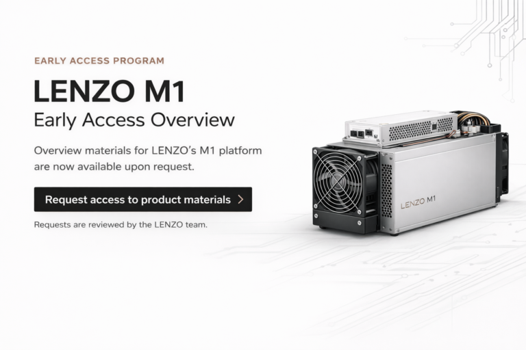
Author - Adrian Sossna

31 Jul

TECHNICAL BRIEF: CGLA: Coarse-Grained Linear Array for Multi-Hash Acceleration in Blockchain Mining

Abstract: In emerging blockchain-based IoT systems, highly flexible and energy-efficient hash function hardware design is necessary to maintain the operation of diverse blockchain networks. Accordingly, a coarse-grained reconfigurable array (CGRA) is the most optimal architecture for implementing hash functions; however, current CGRA-based works still have slow speeds and low energy efficiency.

To solve these problems, this paper proposes a Coarse-Grained Linear Array (CGLA), upgrading from the CGRA, to perform multiple hash functions with high speed and energy efficiency. To achieve that goal, three main ideas are proposed: a self-updating data method, an expandable processing element array (PEA), and an efficient arithmetic logic unit (ALU) dedicated to hash functions. Our CGLA has been successfully implemented on a TySOM-3A FPGA. Evaluations on 45nm ASICs show that the CGLA is 2.8-8.7 times more power efficient than GPUs, and 1.3-17.8 times and 1.9-44.5 times better in throughput and energy efficiency than previous CGRAs.

Contact hello@lenzo.co.jp to request your full copy.


17 Jul

TECHNICAL BRIEF: Bonanza Mine an Ultra Low Voltage Energy Efficient Bitcoin Mining ASIC

Abstract: Bitcoin is the leading blockchain-based cryptocurrency used to facilitate peer-to-peer transactions without relying on a centralized clearing house [1]. The conjoined process of transaction validation and currency minting, known as mining, employs the compute-intensive SHA256 double hash as proof-of-work. The one-way property of SHA256 necessitates a brute-force search by sweeping a 32b random input value called nonce. The 232 nonce space search results in energy-intensive pool operations distributed on high-throughput mining systems, executing parallel nonce searches with candidate Merkle roots.

Energy-efficient custom ASICs are required for cost-effective mining, where energy costs dominate operational expenses, and the number of hash engines integrated on a single die govern platform cost and peak mining throughput [2]. In this paper, we present BonanzaMine, an energy-efficient mining ASIC fabricated in 7nm CMOS (Fig. 21.3.7), featuring: (i) bitcoin-optimized look-ahead message digest datapath resulting in 33% Cdyn reduction compared to conventional SHA256 digest datapath; (ii) a half-frequency scheduler datapath, reducing sequential and clock power by 33%; (iii) 3-phase latch-based design with stretchable non-overlapping clocks, eliminating min-delay paths; (iv) robust ultra-low-voltage operation at 355mV using board-level voltage-stacking; and (v) mining throughput of 137GHash/s at an energy efficiency of 55J/THash.

Contact hello@lenzo.co.jp to request your full copy.


3 Jul

BLOG: CGRA vs. CGLA - Why CGLA is the Better Architecture

In recent years, the evolution of AI has shown no signs of slowing down. Supporting this AI revolution are specialized "AI chips" designed specifically for AI computations. Lately, a growing number of startups developing new AI chips have adopted an architecture called "CGRA."

However, an architecture that solves the major challenges of CGRA and takes things a step further—"CGLA"—remains largely unknown.

This article will explain the difference between CGRA and CGLA for beginners in the semiconductor field, and introduce the advantages and features that give CGLA the potential to dominate the AI era.

What is a CGRA?

Let's start with the basics. What is a CGRA?

In a nutshell, a CGRA (Coarse-Grained Reconfigurable Array) is like a "computer made of LEGO blocks that can be reshaped to fit the program."

If a general-purpose CPU is a "universal factory that can handle any calculation," then a CGRA is like a "specialized factory whose production lines (computing circuits) can be freely reconfigured to make a specific product (perform a specific computation)."

By arranging numerous small processing units and changing their connections according to the program, a CGRA can execute specific tasks like AI image recognition or data analysis overwhelmingly faster and with less power than a CPU.

This is why many AI chip startups are focusing on CGRA. However, this "reconfiguring the production line" process has a major weakness.

The "Major Weakness" of CGRA

The weakness of CGRA is its "compilation time."

Compilation is the process of converting a program written by a human into a blueprint that the hardware can understand. For a CGRA, this is equivalent to figuring out the optimal layout of the production line to achieve maximum efficiency.

Finding the best placement and connection scheme for countless units is like solving an incredibly complex puzzle. As a result, it's not uncommon for CGRA compilation to take several hours, sometimes even more than a full day.

This means that every time you want to try a new AI model or make a small change to a program, it becomes a day-long affair. This is a critical flaw in today's world, where development speed is everything.

Enter the Savior: CGLA

This is where CGLA (Coarse-Grained Linear Array) comes in. As its name suggests, it's an architecture where processing units are connected in a linear—or ring-like—fashion, packed with innovative ideas that solve CGRA's challenges. The "IMAX" from NAIST, mentioned frequently in our chat, is a prime example of a CGLA.

CGLA's Advantage #1: Compilation Time in "Seconds"

Why is CGLA so fast to compile? The secret lies in its namesake "linear (ring-like)" structure.

  • CGRA: Units are arranged in a complex 2D grid, making it very difficult to find the optimal routes.
  • CGLA: Units are connected in a simple ring (linear) structure, which eliminates the need for the compiler to search for complex routes, making the program "mapping" process extremely easy.

This dramatically reduces compilation time from hours to just a few seconds. For developers, this is a revolutionary change.

CGLA's Advantage #2: The Pipeline "Never" Stalls

The biggest drain on a computer's performance is the "pipeline stall," which occurs when the process has to wait for data.

The CGLA (like IMAX) uses the dataflow principle and multithreading technology within its units to eliminate stalls by design.

This is like a factory production line where parts always arrive at the worker's station at the exact moment they are needed. Because the hardware continues to operate without any waste, it maintains extremely high computational efficiency.

CGLA's Advantage #3: Thoroughly Energy-Efficient Design

Moving data is a major source of power consumption. The CGLA (like IMAX) places a large cache memory right next to each processing unit.

This is like each worker on the assembly line having their own personal, large toolbox and parts bin. Since there's no need to constantly walk to a central warehouse for parts, data movement is minimized, leading to significant energy savings.

Summary: CGRA vs. CGLA

Feature

Typical CGRA

CGLA (e.g., IMAX)

Unit Connection

Complex 2D Mesh Structure

Simple Linear (Ring) Structure

Compilation Time

Hours to 1+ Day

Seconds

Pipeline Efficiency

Prone to Stalls

Stall-less

Memory Structure

Frequent access to shared memory

Local cache per unit, minimal data movement

Development Efficiency

Low

Extremely High

As you can see, CGLA is truly a next-generation architecture that refines the CGRA concept and solves its practical challenges.

While startups using CGRA are making waves in the AI chip market today, more advanced technologies like CGLA are steadily moving towards practical application. The day that CGLA—with its combined development efficiency, execution efficiency, and energy savings—becomes the standard for future AI chip development may not be far off.